1, the introduction
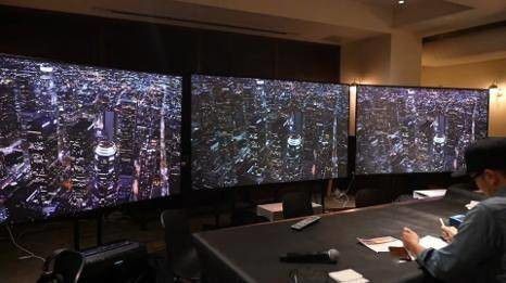
At present, emerging display technologies compete for glory, OLED, Micro LED, QLED, laser display.... Are vying to be the leader in next-generation display technology. Among them, laser display with large gamut, large screen, high resolution, digitalization and other characteristics, is considered to be a strong competitor in the future display technology. Xu Zuyan, academician of the Chinese Academy of Engineering, also said: "The development process of the display industry is from standard definition to high-definition, and is now moving to ultra-high-definition. Laser display technology will certainly become the mainstream technology of the next generation display industry."
In 1966, Korpel et al. [1], Research department of Chicago Zenith Broadcasting Company, proposed the idea of using laser as a display light source for the first time. Subsequently, researchers from all over the world invested in the research tide of laser display one after another. The appearance of laser display technology also provides a new opportunity for the development of display field.
Laser display is moving forward from the traditional technology of blue light + phosphor to the three primary colors of red, green and blue laser display, which is a major breakthrough in colorimetry and solves the problem of large gamut color reproduction which has been pending for a long time in the field of display technology, and can perfectly reproduce natural colors.
Red LD belongs to GaAs material system, blue and green LD belong to GaN material system. Red LD in laser display and other fields of application, need to maintain stable optical mode and laser power output, the life and reliability of the laser requirements are high. The shorter the red LD wavelength is, the higher the optical potential energy is. However, the red laser uses AlGaInP/GaInP structure, and the band-gap difference between the active region and the limiting layer is small, so the limiting ability of injected carriers is poor, and leakage current is easy to be generated. This will not only reduce the internal quantum efficiency and power conversion efficiency of the semiconductor laser, but also lead to lower characteristic temperature of the device and higher sensitivity of output power to temperature. By increasing the dopant concentration in the P-restricted layer, the electron spillage is inhibited. However, at high doping, the dopant diffuses to the active region and the number of defects increases, which affects the reliability of the laser and increases the carrier absorption loss. In order to meet the requirements of screen display, the output power of the laser needs to be increased, which is easy to lead to cavity surface disaster damage (COD). At the same time, in order to enhance the market competitiveness, the wavelength uniformity of epitaxial wafer is required to be good, and the product consistency is put forward higher requirements, so there are very big technical challenges and difficulties in the development of high-power red LD.
This paper mainly introduces the technology development and application trend of the high-power red 638 nm laser as one of the core components of the three-primary color laser display.
2. Technological progress abroad
Red semiconductor laser has the advantages of small size, long life and high electro-optical conversion efficiency. It gradually replaces the traditional HE-NE gas laser and ruby solid laser, and is widely used in CD reading and writing systems, bar code readers, alignment line markers, healthcare equipment and other fields. At the same time, with the continuous improvement of power and performance, it is gradually applied to laser TV, portable projector, landscape lighting and other laser display and lighting equipment [2-4].
Internationally, although Europe and the United States and other developed countries, especially Germany's Osram Company, Ferdinand-Braun Research Institute [5], the United States nLight have a certain amount of investment, red light LD research and development mainly concentrated in several major Japanese electronic companies, including Mitsubishi, USHIO (Oxtail, formerly Hitachi), Sharp, SONY, NEC, Panasonic and so on. The reason for this is that red LD is closely related to home electronic technology, such as the early low-power red LD is mainly used in VCD and DVD, evolution so far, the current laser display and lighting with high-power red laser market is also monopolized by Japanese manufacturers.
The results show that the shorter the wavelength of the red laser larger than 600 nm, the higher the optical efficiency. The longer the wavelength, the greater the range covered by the gamut [3]. According to the standard of National Television Standards Committee (NTSC), when 620 nm red light is selected, the optical performance is 0.33 lm/W, and the color gamut can reach 161%. When 650 nm red light is selected, the color gamut is as high as 211%, and the optical efficiency is reduced to 0.141 lm/W [6]. Therefore, in practical application, it is necessary to comprehensively consider the scene of laser display application and the performance of the light source system to select the appropriate laser wavelength. At present, the red wavelengths used for laser display in the world are usually concentrated at 630 ~ 650 nm, and the 638 nm red semiconductor laser has the highest comprehensive efficiency. But the red laser with short wavelength and high power is a technical difficulty.
SONY demonstrated its 643-nm wavelength high-power semiconductor laser [7] at the International Exhibition of Laser Products and Optical Technology (InterOpto06) held in July 2006, with an output power of up to 3 W. It has been confirmed in the product verification phase that the output power can be increased to 7 W, and the highest output power of this exhibit can also reach 4 W.
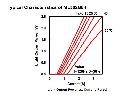
In 2009, Mitsubishi released a 638 nm semiconductor laser for color projectors, and then its output power continued to make breakthroughs. In 2010, it launched a product with a continuous operating power of 500 mW. In 2014, it adopted double luminous spots to increase the continuous output power to 1.8W, and increased the number of luminous spots to 3 in 2015. The pulse output power reaches 2.5W (ML562G84 pulsed red high-power semiconductor laser, performance is shown in Figure 1). In December 2018, ML562G86, a product with 3.0W pulse output power, was released (officially released in April 2019), which became the semiconductor laser with the highest power among the 638nm band lasers reported in that year [8]. Since then, Mitsubishi has no new products of 638nm launched.

Figure 1 Power current curve (pulse) of Mitsubishi 2.5W 638 nm semiconductor laser (model ML562G84)
In 2014, Oclaro introduced 638 nm/700 mW laser diode [9], which is a multi-transverse mode AlGaInP laser. In August 2014, USHIO acquired the Oclaro Semiconductor laser and LED business, which is still used today. In 2017, USHIO successively released two high-power red semiconductor lasers, a single-spot 637 nm/1.2 W (CW)/1.5 W (Pulse) and a dual-spot 638 nm/2.2 W (CW)/2.8 W (Pulse) laser diode. In 2019, USHIO launched A higher power dual spot laser, model HL63520HD, which can achieve 2.4W continuous operating power at 25 ℃ and 2.4A continuous current, while at the pulse condition of 120 Hz frequency, 30% duty cycle and 3.3A current, The pulse operating power can reach 3.5W [10], which is 17% higher than the 3.0W pulse output laser introduced by Mitsubishi in 2018 (see Figure 2), making it the highest power 638nm laser in the world. Since then, USHIO has not released a new 638nm product.
Figure 2 USHIO 638 nm 2.4W (CW)/ 3.5W (Pulse) (HL63520HD) power current curve (CW and Pulse)
3. Domestic technological progress
As early as in the 1980s, China arranged the laser panchromatic display project in the national "863" program, and established the industrial alliance around the laser display technology, aiming to further promote the development of China's laser display industry. In recent years, the Ministry of Science and Technology, through the national key research and development plan, has concentrated the advantageous resources, arranged the three primary color light source and other key components and the whole machine for research and development, and achieved fruitful results. At present, China leads the world in the number of laser display patent applications, and has the most comprehensive patent layout, covering the light source, control, optical machine, machine and optical components, and has initially formed a patent pool.
In terms of research, non-absorption window, cavity surface passivation, large optical cavity structure, current non-injection window and other key technologies can effectively suppress the COMD phenomenon and improve the single-tube output power of the device.
In 2018, Shandong Huaguang Zhu Zhen et al. [11] replaced the original gaseous Zn expansion method with the solid-state Zn expansion method to improve the stability and repeatability of the non-absorption window process, and prepared a 660 nm semiconductor laser with a continuous output power up to 4.2W. In 2019, Xia Wei et al. [12] from the University of Jinan prepared a 640 nm semiconductor laser with a width of 100 μm and a cavity length of 1.5 mm and compared its performance on heat sink materials with different thermal conductivity. At room temperature of 25℃, the thermal resistance of the device is about 9.1 K/W, the threshold current is 0.45 A, and the maximum output power can reach 2.9 W. When the chip is packaged on SiC heat sink with higher thermal conductivity, the thermal resistance of the device decreases to 5.6 K/W, the threshold current decreases to 0.42 A, and the maximum output power increases to 3.9W, an increase of 34.5%. In 2020, Huaguang produced a 640nm laser chip with a width of 40μm and a cavity length of 1500μm, which was finally packaged into TO5.6. At room temperature, the TO device generated more than 600mW of power under the 1A test current, with a maximum conversion efficiency of 25%.
Shenzhen Raybow Optoelectronics Co., LTD., as one of the few companies in China that develop and produce high-power semiconductor laser chips, has participated in and undertaken all six topics related to the red light display source in the 2016-2018 key R&D plan of the Ministry of Science and Technology since 2016. In 2017, it is the general leader of the key research and development program of "High beam quality, low threshold, long life, low cost red LD material and device key technologies and engineering research". At present, after years of hard research and development, the 638 nm laser chip of Raywave Optoelectronics has overcome a number of key technologies such as quantum well hybrid, non-absorption window and cavity surface passivation, and successfully introduced into mass production and marketing. At present, there are 0.5W, 1W, 2.5W 638 nm chips and 2W 665 nm chips in mass production.
The 1W 638nm chip adopts a size structure with a strip width of 110μm and a cavity length of 1.5mm (see Figure 3), while the 2.5W 638nm chip adopts a size structure with three luminescent points, each with a strip width of 60μm and a cavity length of 1.5mm (see Figure 4).

FIG. 3 Single spot, strip width 110μm structure

FIG. 4 Three luminescent points, strip width 60μm×3 structure
Ripple also developed 665 nm single spot, 40μm width and 110μm width red LD. Due to the longer wavelength, the photoelectric performance of 665 nm red LD is significantly better than that of 640 nm red LD. Because the global high-power red light LD market is mainly monopolized by Japanese manufacturers, the representative manufacturers are Mitsubishi, USHIO and Sharp, among which Mitsubishi products are the most advanced and the market share is the largest. Since Mitsubishi does not have a chip with a luminescent strip width of 110μm, the 500 mW 40μm red light LD is compared with the 50μm red light LD of Mitsubishi's approximate specification (product model ML501P73, specification is 500 mW), as shown in the table below, and the performance comparison is shown in Figure 5.
Comparison table of Performance parameters between Raywave and Mitsubishi Red Light Chip (1.5mm cavity length, 40μm strip width)
FIG.5 PI curve comparison of Raywave and Mitsubishi Red Light chip at 25℃ and CW (1.5mm cavity length, 40μm width)
From the current comparison results of the two sides, the T0 temperature parameters of the commercialized Mitsubishi 500 mW red LD are consistent with the red LD manufactured in bulk by Ripple, and the wavelength is also consistent. However, the red LD of Ripple Photoelectric is slightly better in the output power, which can be said to have reached the world's leading position in the core index. At the same time, the 638 nm multi-spot chip and 665 nm chip developed by Ripple also fill the domestic gap in performance and reach the forefront of the world.
4. Trends and Prospects
Over the past 20 years, the laser demonstration in our country has experienced three development stages from principle feasible, technology feasible to industry feasible. By 2019, there were more than 100 enterprises in the upstream and downstream industrial chain of laser display, with an annual output value of more than 15 billion yuan.
In the current display market, although the output of liquid crystal panels in mainland China has ranked among the top in the world, industry data show that only in the upstream of the panel material industry, including polarizer, glass substrate, target material, photomask, photoresist and other products, the localization rate does not exceed 20%.
The laser display field has formed industrial advantages, the localization rate is now in the range of 45%-55%, the development space is huge. The localization of core devices and components has been fully carried out, and it is expected that the proportion of localization will be increased to 75%-80% in 3 years.
Laser TV is a TV product with a high degree of independent research and development in the history of Chinese television. In the history of global display industry, this is a beautiful "lane change overtaking" of Chinese enterprises. In the long term, the steady shipment level of laser TV in China or 6 million units, and if considering the penetration of laser TV to commercial scenes and the global market, the long-term development space will be broader. Because has the larger technology growth space and the obvious technology route advantage, the laser television attracted many giants to enter quietly.
Home appliance giant Hisense has been deploying laser displays since 2007. As of June 30, 2021, it had applied for 1,439 domestic and foreign patents in the field of laser display, and granted 575 patents, laying a solid foundation for the upgrade of laser display.

Figure 6 Hisense Panchromatic laser TV L9G was named "King of Laser ultra-short focus Products" in 2021 (the far left is Hisense laser TV L9G, using RGB three-color laser light source, reaching 3000 lumens) Source: Sohu
In addition, Changhong has completed the all-channel, serialized laser display product layout. Xiaomi, Baidu, Ali have directly or indirectly into the laser TV field; Guangfeng Optoelectronics went public in 2019, raising 1 billion yuan to devote to the development of laser display; Zhongke Aurora completed a new round of financing... More giants are jumping on the bandwagon, focusing on research and development to get a head start on the new track.
In addition, this year, laser display in the application boundary began to penetrate into a larger "segment" - intelligent micro investment market, dimensionality reduction hit. In terms of volume, the annual smart home projection market is expected to exceed 4 million units in 2021, which will be the "segment" of the projection industry highlight. Generally speaking, the requirements of red laser chip for laser projection/display applications are high power, high reliability, good consistency, etc. Generally, certain temperature control measures are taken to control the operating temperature of the chip.
In addition, red laser in the field of lighting (stage/landscape/car (Figure 7)), medical beauty (photodynamic therapy PDT (Figure 8), hair growth and transplantation, etc.) have shown good application opportunities. Among them, laser lighting requirements for 638nm high temperature resistance characteristics are good, generally adopt air cooling, so the requirements of high temperature working conditions of high power stability, decline reduction, which is different from the projection application requirements. The wavelength of medical beauty/germinal hair is generally 650nm and 665nm, and the difference shows the application of 638nm wave

